
Profiler Permukaan Stylus Profesional
A Professional Stylus Surface Profiler is a high-precision measurement instrument designed for accurate surface roughness and profile analysis of industrial components. The Professional Stylus Surface Profiler uses a diamond stylus sensor to trace micro-surface variations with exceptional resolution, converting physical surface texture into precise digital data. The Professional Stylus Surface Profiler is ideal for applications requiring strict surface quality evaluation and repeatable measurement accuracy in modern manufacturing environments.
- Pengukuran: Teknologi profil probe
- Probe Sensor: Low inertia sensor (LIS3)
- Tekanan Probe: Using LIS3 sensor: 1 to 15mg
- Tampilan Sampel: Selectable magnification, 1 to 4mm FOV
Deskripsi Produk
The Professional Stylus Surface Profiler integrates advanced measurement technology with a stable and user-friendly platform, delivering precise surface characterization for modern laboratories and production environments. It offers excellent accuracy, reliable repeatability, and efficient operation, making it suitable for both research and industrial quality control applications.
Designed for high-resolution surface analysis, this system supports nanoscale roughness, step height, and 3D topography measurement. It is widely used in microelectronics, semikonduktor, display manufacturing, solar energy, perangkat medis, and advanced materials research, helping users achieve superior process control from R&D to final inspection.
Professional Stylus Surface Profiler – Nanometer-Level Step Height & Surface Roughness Measurement
The Professional Stylus Surface Profiler is a high-precision contact measurement system designed for accurate analysis of step height, kekasaran permukaan, and 3D surface topography. Using a diamond stylus that gently traces the sample surface, it captures fine surface variations with exceptional resolution and stability. This ensures highly reliable and repeatable measurement results for demanding industrial and laboratory applications.
Cara Kerjanya
The system operates based on a contact-style measurement method. As the stylus moves along the surface, its vertical displacement mirrors the surface contours. This movement is captured as an electrical signal through a measuring bridge, generating an amplitude-modulated output proportional to the vertical displacement. The signal is then amplified, processed through phase-sensitive rectification, and filtered to remove noise and waviness. This ensures that the final output is a clean and stable signal, providing accurate step height and roughness measurements free from external interference and waviness.
Aplikasi Utama
- Semiconductor Wafer Metrology: Precise measurement and analysis of semiconductor wafers to ensure high-quality fabrication.
- MEMS and Microstructures: Accurate profiling of MEMS (Micro-Electro-Mechanical Systems) and microstructures for detailed surface measurements.
- Thin Film and Coating Thickness: Evaluation of the thickness and uniformity of thin films and coatings, critical for various manufacturing processes.
- Solar Cell Surface Profiling: Accurate surface measurements for solar cells, optimizing performance and manufacturing quality.
- Precision Optics and Medical Devices: Measurement of precision optics and medical devices to maintain high standards of quality and performance.
Fitur utama
- Stable Performance: Ensures consistent operation with fast transmission, automatic calibration, and accurate measurement.
- Revolutionary Desktop Design: Achieves a balance of high performance, ease of use, and cost-effectiveness in a compact benchtop setup.
- Compact & Reliable Design: Optimized hardware configuration ensures high testing accuracy, stabilitas, and efficiency.
- Superior Materials & Daya tahan: Crafted with high-quality materials to ensure durability, masa pakai panjang, and efficient performance.
Fitur Peralatan
- Unrivaled Performance: Step height reproducibility below 4A, with enhanced scanning capabilities.
- Single-Arch Design: Provides breakthrough stability, minimizing ambient noise interference, and enabling a large vertical range with low-force scanning.
- Upgraded Smart Electronics: Reduces noise and enhances measurement accuracy, capable of measuring step heights below 10nm.
- Optimized Hardware Configuration: Reduces data acquisition time by 40%, improving measurement efficiency.
- 64-bit Vision64 Synchronous Software: Accelerates data processing, increasing data analysis speed by 10x.
- Intuitive User Interface: Vision64 software offers a simplified, user-friendly interface for easier setup and analysis.
- Automatic Tip Alignment System: Simplifies probe changes with self-aligning probe assembly, reducing risks during transition.
- Wide Range of Probe Models: Offers various probe sizes and shapes, ensuring compatibility with nearly any application.
- Single Sensor Design: Delivers low-force measurements with a wide scanning range on a single plane.
- High Throughput Testing: Ensures quick, multi-sample testing for precise thin film measurements with superior repeatability.
Parameter teknis
| Teknologi Pengukuran | Teknologi profil probe |
| Fungsi Pengukuran | Pengukuran profil permukaan 2D |
| Pengukuran 3D opsional/ | |
| Tampilan Sampel | Selectable magnification, 1 to 4mm FOV |
| Probe Sensor | Low inertia sensor (LIS3) |
| Tekanan Probe | Using LIS3 sensor: 1 to 15mg |
| Low Force (Opsional) | Using N-Lite+ low force sensor: 0.03 to 15mg |
| Opsi Probe | Probe curvature radius selectable range: 50nm to 25μm; |
| Height-to-diameter ratio (HAR) tips: 10μm*2μm and 200μm*20μm; | |
| Custom tips are available upon request. | |
| Contoh Tahap X/Y | Manual X-Y translation: 100mm (4 inches) |
| Motorized X-Y translation: 150mm (6 inches) | |
| Contoh Tahap Putar | Manual, 360° rotation; |
| Motorized: 360° rotation; | |
| Sistem Komputer | 64-bit multi-core line processor, Windows* 7.0; Optional 23-inch flat panel display |
| Perangkat lunak | Vision64 operation and analysis software; |
| Stress measurement software: Cantilever deflection; | |
| Suturing software: 3D scanning imaging software | |
| Perangkat Peredam Getaran | Redaman guncangan tersedia |
| Rentang Panjang Pindai | 55mm (2 inches) |
| Titik data per pemindaian | Up to 120,000 data points |
| Ketebalan sampel maksimum | 50mm (2 inches) |
| Ukuran wafer maksimum | 200mm (8 inches) |
| Reproduktifitas tinggi langkah | <4A1σ on a 1μm step |
| Rentang Vertikal | 1mm (0.039 inches) |
| Resolusi Vertikal | Maximum 1A (at 6.55μm vertical range) |
| Masukan Voltage | 100 - 240 VAC, 50 - 60Hz |
| Kisaran Suhu | Operating Range 20 to 25°C (68 to 77°F) |
| Kisaran Kelembaban | ≤80%, Non-condensing |
| Ukuran dan berat sistem | 455mm W x 550mm D x 370mm H |
| (179in. W x 22.6in. D x 14.5in. H); | |
| 34 kg (75 lbs); | |
| Attachment: 550mm L x 585mm W x 445mm H (216in. L x 23in. W x 175in. H); | |
| 217 kg (48 lbs) |
Kasus Aplikasi
- Thin Film Testing – Ensuring High Yields:
In semiconductor manufacturing, Step instrument helps monitor deposition and etching uniformity, thin film stress, and ITO thin film thickness. Its high reproducibility ensures accurate measurement, optimizing etching and deposition for better yields. - Surface Roughness Inspection – Ensuring Performance:
Ideal for assessing surface roughness in precision components across industries like automotive, kedirgantaraan, and medical devices. Misalnya, it measures the roughness of orthopedic implant coatings to ensure product quality and adhesion. - Solar Grid Line Analysis – Reducing Manufacturing Costs:
Perfect for measuring the dimensions of conductive silver grid lines on solar panels. Step instrument ensures that silver usage is optimized for better conductivity, contributing to cost-saving in solar panel production. - Microfluidics Technology – Detecting Design and Performance:
Used in MEMS and microfluidics technology for qualification testing. The low-force NLite+ measurement function enables precise detection of vertical steps and roughness on photosensitive materials, ensuring design accuracy and performance.
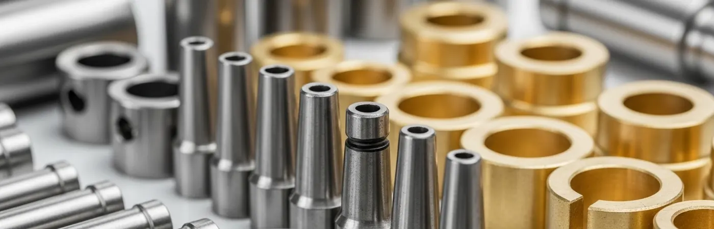
Mulailah dengan solusi Anda hari ini!
Apakah Anda mencari mesin CNC berperforma tinggi atau mesin manual yang andal, Kami menawarkan solusi yang disesuaikan untuk memenuhi kebutuhan spesifik Anda.
Hubungi kami hari ini untuk mendiskusikan kebutuhan Anda dan mendapatkan saran ahli. Biarkan kami membantu Anda mengoptimalkan proses manufaktur Anda!
Keuntungan kami
Didukung oleh pengalaman teknik lebih dari 25 tahun, Tim kami menawarkan layanan komprehensif—mulai dari desain cetakan yang disesuaikan dan pemesinan presisi hingga produksi skala penuh—didukung oleh sistem jaminan kualitas yang kuat dan layanan pelanggan yang proaktif. Bersertifikat di bawah ISO9001, ISO14001, dan IATF 16949, Kami terus berupaya mencapai keunggulan dalam kualitas, inovasi, dan kepuasan pelanggan.
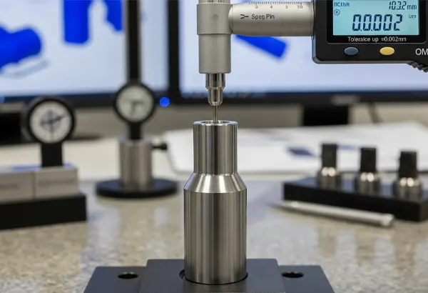
Presisi Toleransi Hingga ±0.002mm
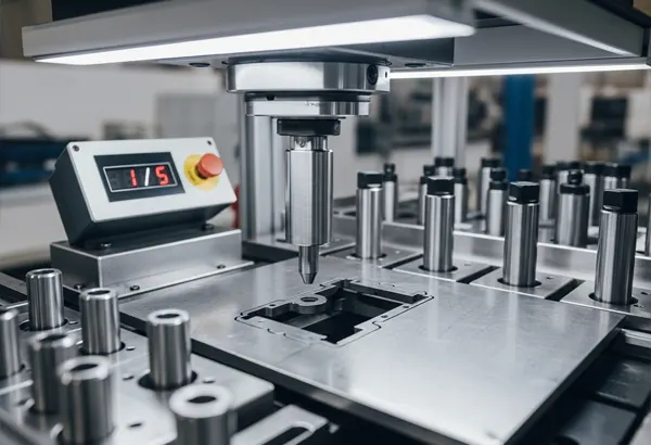
Bahan asli pilihan 1 buah setara dengan 5 buah
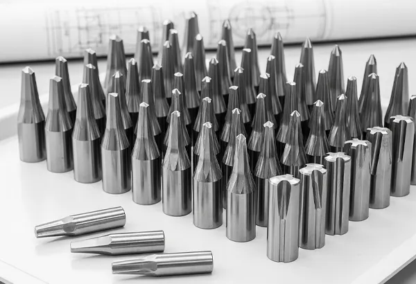
Pemrosesan batch dan kustomisasi berdasarkan gambar, pengambilan sampel bebas.
Rentang Aplikasi
Pilihan utama di berbagai industri.